- A team led by Nanjing University used a methylammonium thiocyanate (MASCN) post-treatment to “heal” perovskite films on industrial textured silicon.
- The tandem cell reached a certified stabilized efficiency of 30.77% and held its initial performance through 3,400 hours of continuous maximum-power tracking.
- The real prize is durability: the treatment tackles the defect and interface problems that have held perovskite tandems back from commercial production.
Solar researchers have chased the perovskite-silicon tandem cell for a decade because the math is irresistible. Silicon converts sunlight well but caps out near 29% efficiency on its own. Stacking a perovskite layer on top captures parts of the spectrum silicon wastes, and the combination can push well past 33%. The catch has never been the concept; it has been keeping the perovskite layer intact and efficient for years, not weeks.
A team led by Nanjing University, with researchers from Renshine Solar, Yunnan University, Zhejiang’s laser intelligent equipment innovation center, and Sweden’s Uppsala University, has now demonstrated an approach that moves the stability needle meaningfully. Their tandem cell posted a certified stabilized efficiency of 30.77% — and, more significantly, an encapsulated device retained its initial performance after 3,400 hours of continuous operation at maximum power point under one-sun illumination in ambient air.
The findings were published in Nature Communications in a paper titled “Healing intervention for improving the efficiency and stability of tandem devices on industrial textured silicon.”
A simple treatment, an awkward surface
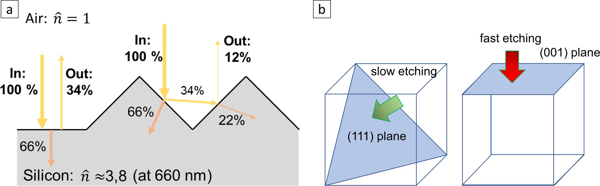
The manufacturing detail that matters most here is the substrate: industrial textured silicon. Commercial silicon wafers are etched with microscopic pyramids that trap light, and virtually all mainstream production uses this texture. But those same pyramids make it difficult to deposit a smooth, defect-free perovskite film. Coverage gaps and small, defective grains pile up on the taller pyramids, and the usual crystallization tricks that work on flat glass simply don’t transfer to the bumpy surface.
The team’s fix is refreshingly low-drama. Instead of reformulating the deposition chemistry, they apply a methylammonium thiocyanate (MASCN) solution to the perovskite film after it has already formed. This “healing intervention” triggers secondary crystal growth through Ostwald ripening — small grains dissolve and feed larger ones — producing large, conformal columnar grains that extend through the full film thickness. Grain boundaries, the defect hotspots that drive non-radiative recombination and sap voltage, are largely eliminated.
Using in-situ SEM, X-ray diffraction, and photoluminescence measurements, the researchers traced how the treatment solution penetrates the underlying film and re-forms it from within, confirming conformal coverage across the textured surface. The method was demonstrated on n-type silicon wafers textured on both sides, using a hybrid two-step process: lead iodide and cesium bromide co-evaporated onto the silicon, followed by a spin-coated layer of formamidinium iodide and bromide.
The numbers, in context
The treated 1.68 eV wide-bandgap perovskite top cell reached 21.1% champion efficiency on its own. Combined with the silicon bottom cell, the tandem device was independently certified at 30.77% with an open-circuit voltage of 1.915 V, a short-circuit current density of 20.13 mA/cm², and a fill factor of 79.85% over a 1.164 cm² active area, with negligible hysteresis, perovskite-info’s analysis of the paper notes.
How does that stack up? The paper itself provides the comparison: for the industry-standard textured silicon (pyramids taller than 1 µm) combined with the hybrid two-step deposition method, the previous certified best was 31.6% — while the same approach on submicron-textured silicon, which the industry doesn’t use at scale, had reached 34.58%. The new 30.77% figure therefore lands within striking distance of the ceiling for this manufacturing-relevant combination. And the researchers describe the 3,400-hour stability result — the device retained its full initial performance — as the best stability reported to date for a perovskite/silicon tandem cell. For a technology whose entire commercialization story hinges on surviving decades outdoors, that is arguably the more important number.
“The resulting 1.68 eV wide-bandgap perovskite solar cells achieve a champion efficiency of 21.1%, contributing to a certified stabilized tandem efficiency of 30.77% and an impressive open-circuit voltage of 1.915 V over an active area of 1.164 cm². Notably, an encapsulated device retains its initial performance after 3,400 hours of continuous maximum power point tracking under one-sun illumination in ambient conditions, representing the excellent stability in perovskite/silicon tandem cells reported to date.” — the research team, via pv magazine
Why this matters for manufacturing
There are two reasons industrial textured silicon keeps appearing in these announcements. First, compatibility: a tandem process that works on the texture the industry already uses can slot into existing cell lines rather than demanding an entirely new manufacturing stack. Second, the scale problem is real — RenShine Solar reported a 26.4% TÜV SÜD-certified all-perovskite tandem module at 809 cm² in September 2026, suggesting laboratory tricks are beginning to survive the jump toward commercial dimensions.
The MASCN healing approach fits that trajectory. It’s a post-treatment, not a new deposition regime, which makes it comparatively easy to bolt onto existing process flows. The mechanism — Ostwald ripening driven by a thiocyanate additive — is also well understood from earlier flat-substrate work; the novelty is in getting it to work on the micron-scale pyramids of production silicon.
What comes next
Several hurdles remain before tandems appear on rooftops. The paper’s devices are centimeter-scale, far from the ~200 cm² cells of commercial panels. Long-term outdoor stability — humidity, thermal cycling, UV — still needs to be demonstrated over timescales that match the 25-year warranties buyers expect. And the industry’s ongoing transition to new silicon cell architectures means tandem processes will need to track a moving manufacturing target.
But the direction of travel is clear. Tandem announcements in 2026 have shifted from “can we build it?” to “can we keep it alive?” — and this paper answers that second question with unusual rigor: 3,400 hours of continuous maximum-power tracking is roughly four months of non-stop noon sun, and the device didn’t budge. For a technology once dismissed as a lab curiosity that would dissolve in a rainstorm, that’s worth paying attention to.